 Naxau Vacuum Coating Processing - Naxau AM
Array
Magnetron sputtering - dual magnetron and intermediate frequency magnetron sputtering
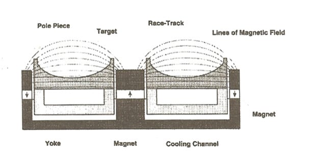
High deposition rates and target utilization are important for industrial processes. Although the deposition rates for magnetron cathodes are relatively high, they are not as high as those for evaporation processes (addressed in previous blogs). Dual magnetron/pulsed magnetron configurations can achieve both high deposition rates and improved material utilization [1,2,3]. Dual magnetron sputtering uses an intermediate frequency (~40 kHz - 300 kHz) pulsed power supply and two magnetron cathodes. The dual magnetron configuration is shown in Figure 2 and a typical power supply pulse is shown in Figure 3. The power supply delivers a positive pulse to one magnetron cathode while negatively biasing the other cathode for the first half of the cycle, and then delivers a positive pulse to the other magnetron cathode while negatively biasing the other cathode. In this manner, one cathode acts as the anode while the other cathode acts as the sputtering cathode. Sputtering occurs only during the negative bias. This process is well suited for reactive sputtering [4,5,6].

Pulsed magnetron sputtering overcomes two disadvantages of magnetron sputtering:
- Anodes are lost (or hidden) due to deposition of insulating layers
- Charging and Arc Formation during Reactive Sputtering
Charging of the target during reactive deposition is practically eliminated due to the inversion of the pulsed power supply and pulse polarity. Figure 4 shows the plasma switching during dual magnetron sputtering [2].

Dual magnetron techniques were initially developed to deposit insulating materials such as oxides, nitrides and transparent conducting oxides [4]. Planar magnetrons with the same target are usually placed next to each other, but in co-sputtering configurations with different targets can be farther apart [5]. Arcing can be reduced by secondary electrons emitted from the negatively biased target (cathode) being attracted to the positively charged target (anode) and essentially neutralizing the positively charged surface of the deposited insulator. Table 1 compares the deposition rates and optical properties of four materials deposited by conventional DC magnetron sputtering and IF sputtering [1,2]. In all cases, we can see that the deposition rate can be increased by up to a factor of 5.

Other thin film materials that benefit from MF dual magnetron sputtering are SiO2, Al2O3, MgO, CrN, ITO.
Let us look in more detail at reactive sputtering, which is one of the advantages of the dual magnetron process. The basic mechanism behind reactive sputtering is complex and still under investigation [7,8], but dual magnetron sputtering makes the process easier to control [6,9]. In addition, closed-loop controllers can be used to automate the process [6]. Target oxidation or poisoning is the main problem that reduces the deposition rate, causes arcing and reduces density. The trick to reactive sputtering is to keep the target surface clean and prevent "anode disappearance", which is directly related to controlling the partial pressure of the reactive gas. For conventional magnetrons, this is accomplished by plotting the hysteresis loop of the reactive gas partial pressure and reactive gas flow, as shown in Figure 5 [10]. The optical properties depend on the deposition rate and the reactive gas partial pressure, as shown in Fig. 6 [10,11]. Initially, the surface reaction with the metal target consumes a large amount of reactive gas. After saturation of the reaction, the target surface will be oxidized and no additional reactive gases will be consumed, therefore, O2Even at lower flow rates, the partial pressure increases. When this occurs, the deposition rate is greatly reduced. Once the target is fully poisoned, O 2'sThe partial pressure will increase linearly with flow. In this case, the flow control and deposition process should be in the negative slope region.


The hysteresis curves for dual magnetron sputtering appear to be nearly identical, but most IF systems use some form of closed-loop or plasma emission monitor control to maintain the partial pressure and flow rate of the reaction gas at optimum values [1,6,9]. Several companies sell closed-loop controllers. An example of a chamber configuration is shown in Fig. 7 [6]. The system uses a set point for the target voltage and a very fast flux control value to keep pace with the chemical reactions occurring on the target surface. In short, the controller compares the target voltage during deposition to the setpoint and adjusts the reactive gas flow accordingly.

The advantage of using dual magnetrons and an IF power supply for co-sputtering is that the amount of each component can be precisely controlled [5]. Obviously, two magnetrons are required for this process, but the use of an IF power supply allows the power supplied to each target to be regulated reliably and independently for each target. This leads to more control over the relative composition. Figure 8 [5] shows a co-sputtering setup using an IF power supply. This configuration was used for co-sputtering using Ti and Al targets as well as O 2The reactive gases come from defining TiAlO xThe refractive index of the FIG. 9 illustrates how the refractive index can be adjusted by adjusting the O 2Partial pressure to control refractive index.


Dual magnetron sputtering can also be used to deposit optical multilayer coatings [9], TCO's [4,12] and friction coatings [13]. Using dual magnetron deposition as shown in Fig. 10 for SiO 2 / Al 2 o 3antireflection coating and then moving the substrate sequentially on each target. The resistivity and optical transmittance of the ITO films were found to be dependent on the pulse length and plasma density as well as conventional parameters such as O 2partial pressure and the power reaching the target [12]. Using two In 0.9 Sn 0.1The ITO resistivity of the process, the pulse length and the O 2The objective of the relationship between the flows is shown in Fig. 11 [12]. Here, we see that very respectable values around 5 mΩ.cm are obtained, with a large dependence on the pulse length.


Because two targets are used, nanolaminates and nanocomposites can also be deposited using dual magnetrons [3,13]. Fig. 12 shows the use of an RF power supply to deposit Al 2 o 3 -ZrO 2High resolution bright field TEM of nanocomposites [3]. The introduction of ZrO2 nanoclusters to enhance the Al 2 o 3Corrosion resistance of TiN / TaN. x(See this month's column.) Multilayers have tribological applications. Multilayers were deposited in Ar + N2 mixtures using Ti and Ta targets [13]. The periodicity of the power supply naturally forms nanolayers of each composition. It is important to control the stresses in these films to minimize flaking and loss of adhesion. Stress in multilayer structures can be controlled by the thickness of the laminate and the partial pressure of nitrogen (which also affects the deposition rate). Figure 13 shows the effect of stress on layer thickness and total pressure (Ar + N 2, the Ar pressure is kept constant) dependence. Adjustment of these parameters allows the stress to change from compressive to tensile.


A list of examples of dual magnetron and IF sputtering can fill several Blogs. using RF as well as IF power to deposit thin films. Cathode magnetic interactions can also be a problem when the cathodes are placed side by side [1]. Each case is different and the cathode configuration must be adjusted to the desired substrate geometry, composition and properties.
Go to http://vtcmagblog.com/
Reference:
- U Heister et al., 41st Annual Technical Conference Proceedings of the Society of Vacuum Coaters (1998) 187.
- T Winkler, 45th Annual Technical Conference Proceedings of the Society of Vacuum Coaters (2002) 315.
- D H Trinh et al., J. Vac. Sci. Technol. A 24(2) (2006) 309.
- W-M Gnehr et al., 48th Annual Technical Conference Proceedings of the Society of Vacuum Coaters (2005) 312.
- D J Christie et al., 46th Annual Technical Conference Proceedings of the Society of Vacuum Coaters (2003) 393.
- L Lou et al, Advanced Energy Industries, Inc. Whitepaper.
- R DeGryse et al., VT&C February 2008, 48.
- W D Sproul, 36th Annual Technical Conference Proceedings of the Society of Vacuum Coaters (1993) 504.
- J Strumpfel et al., 40th Annual Technical Conference Proceedings of the Society of Vacuum Coaters (1997) 179.
- W D Sproul et al., J. Vac. Sci. Technol. A 13(3) (1995) 1198.
- W D Sproul and B E Sylvia, VT&C, 2(8) (2001) 32.
- A I Rogozin et al., J. Vac. Sci. Technol. A 22(2) (2004) 349
- M Nordin et al., J. Vac. Sci. Technol. A 18(6) (2000) 2884.